CO 7. DesignofProcessor
Last Edit: 3/10/26
The former course is about to use Assembly and C language to view the processor in terms of a programmer, now the course has been switched into view processor hardware using digital design knowledge
Computer Architecture #
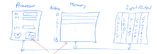
Recall the architecture we have, what the processor does is
- Fetch from the memory to get Machine Code instructions
- Execute the instructions
- Interact with memory
Now we are going to use logic gates to rebuild this
Simple Processor Design #
The processor we are working on will be a 8 bit one, with one 4 Registers, R0 - R3
- By setting the processor to 8 bit, it means that its word size is 8 bits
- As the memory address also only have 8 bits, thus there’ll be $2^8=256$ memories
- The same applies to
pc
Instruction Set #
There’s gonna be 10 kinds of instruction, with also fixed size of 8 bits
- And the instruction is going to look like
add R1, R2 # R1 = R1 + R2
Condition Flags #
There’s going to be two 1 bits flag
- Z Bit (Zero): If the last instruction result is zero,
z = 1, else isz = 0 - N Bit (Negative): If the last instruction result is negative,
N = 1, elseN = 0
Nios V doesn’t use this method
Datapath #
Before starting, here’s some part of the processor that we have to get
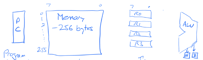
- PC
- Memory
- Register
- ALU
Data Flows #
Fetch Path #
- Starting from
pc, it send the required address tomemory - Then
memoryoutput the Instruction toInstruction RegisterandMemory Data Register
Execution Path #
- Then
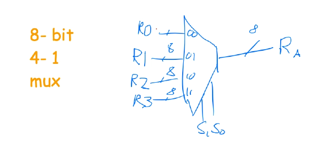
Register Filewill choose to read one ofregAandregB - Then using
Multiplexersto decided which data to pass through - Lastly use
ALUto get the final result
Instruction Formats #
As indicated, there’s 8 kinds of instructions, where they can be extracted into two types
Reg - Reg ones #
The operation between two Registers, i.e. add R1, R2 , inside the instruction, there will be
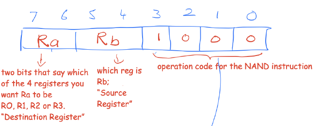
Opcode(4 bits): Choosing operationregA(2 bits): Target RegisterregB(2 bits): Source Register
Immediate ones #
The operation between Register and Constants, i.e. addi R1, 5
Opcode(4 bits): Choosing OperationregA(2 bits): Target RegisterregB(2 bits): Immediate Number (Notice the range is $2^2$ which is $0-4$
Semantics #
Regardless of add Ra, Rb or sub Ra, Rb , they are having similar operations
Arithmetic Operation #
Calculate the operation result first
Flags #
Then update two status bits, Zero and Negative
Then update pc = pc + 1
Encoding of Machine Code #
One instruction will be extract into three parts in a 8 bit Register
Or immediate Operation #
The General Form of Or Immediate Operation is ori imm5 , notice
- There’s NO Given Register for this command
- There’s 5 bits on immediate number
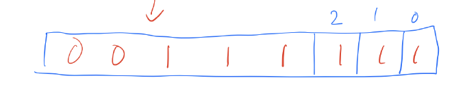
Firstly the Register issue, we fix the Register of this operation to R1 to save two 2 bit of space
Secondly, as there’s only 3 bits for Opcode and it’s 111 ,thus we have 5 bits for this constant
Execution Steps #
- $R1 \leftarrow R1 \ OR \ ZE(Imm5)$
- Here
ZEmeans Zero Extend, add three zero in front of 5 immediate to make it 8 bits
- Here
- Update the
ZandNbit - Update
PC: $PC \leftarrow PC + 1$
Ex. ori 0x7 #
Memory Instructions #
There’s two Memory Instructions used load and store , it’s similar to lw and sw , but notice for the Memory Instructions, the Z and N bit won’t be set as there’s no ALU logic
Load Operation #
The general form of Load Operation is load Ra, (Rb) , and will be encoded in the form of

Store Operation #
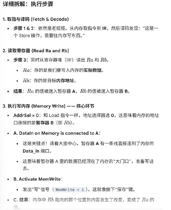
The general form of Store Operations is store Ra, (Rb) , will be encoded in the form of

Conditional Branches #
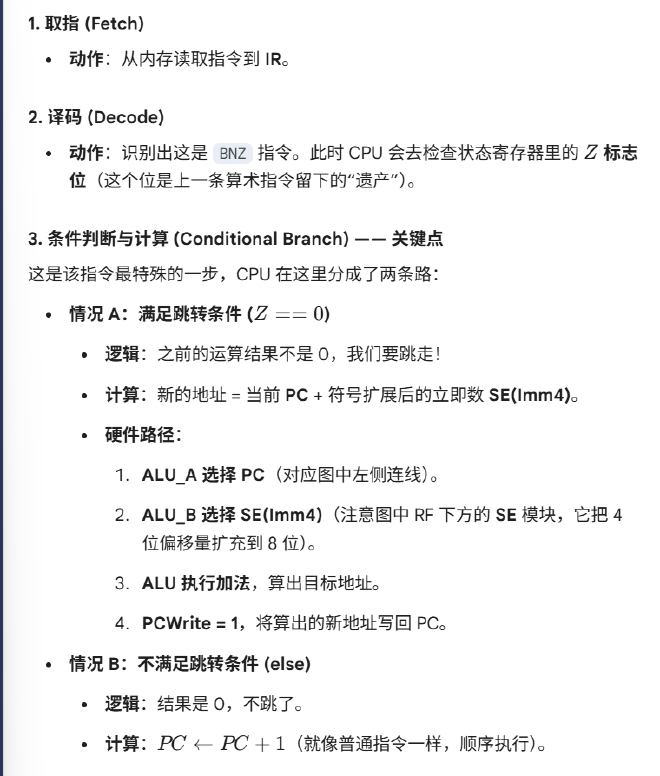
Recall the instruction bne r5, r0, loop , this is a branch if not zero instruction, that branch to a different address (other than pc+1) if result of last operation in ALU is not zero
In this Simple Processor, we can tell this by using the Z bit, thus here’s the full step for Branch
Running the instruction bnz Imm4
- Check the
Zbit, ifZ == 0(The result is not zero), then JUMP- If
Z == 1(The result is zero), thenPC <- PC + 1
- If
- Jumping process is using an offset that
PC <- PC + SE(Imm4), hereSEis Sign Extension - Here we are using Relative Addressing
This having the Encoding of
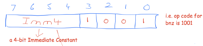
There’s up four bits for Imm4 - 4 bits constant, and lower 4 bits Opcode with bnz = 1001
While there’s also an Instruction bpz imm4 which is Branch if Positive with Opcode of 1101
Design Example #
Here’s a full code comparing two value in Memory and see if they subtract to zero
| Address | Label | Instruction | Comment | Encoding |
|---|---|---|---|---|
| 0 | loop: | load R2,(R0) |
R2 <- [R0] |
0x80 |
| 1 | load R3,(R1) |
R3 <- [R1] |
0xd0 |
|
| 2 | sub R2, R3 |
R2 <- R2 - R3 |
0xb6 |
|
| 3 | bnz loop |
0xd9 |
The hardest thing here is to calculate Imm4 for Encoding bnz , notice loop is at address 0 , when running til bnz loop , PC is already 3 m thus we want
$$ PC + Imm4 = Target\rightarrow3 + Imm4 = 0 $$
Thus we get $Imm4 = -3$, in 2’s Complement, -3 is just 1101 , thus this Encoding code will be 1101 1001 = 0xd9
Register #
Recall the implementation of a Register, its fundamental unit is a D Flip-Flop
D Flip-Flop #
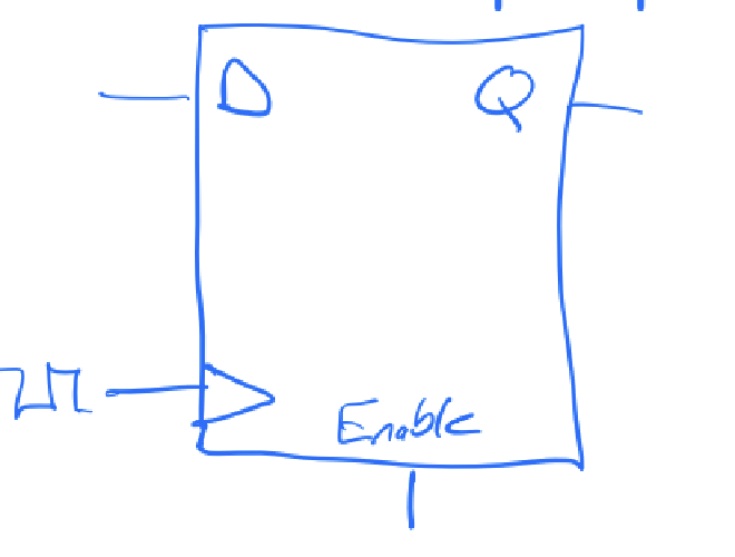
This Flip-Flop contains an input D, output Q, clock and a Enable , this Flip-Flop will update when there’s a positive edge of clock, then check if Enable = 1 , then Q <- D , otherwise the output Q will remains the same
In this Processor, as we indicated is a 8 bit register, there’s gonna be 8 Flip-Flops together, sharing the same Enable and Clock
The Clock ’s frequency depends on the device we are running at, its $50MHz$ for Nios V, and $2GHz$ for normal computers
Multiplexer #
Instructions #
add #
Recall the execution of the add instruction add Ra, Rb # Ra <- Ra + Rb , with the encoding of
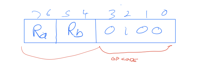
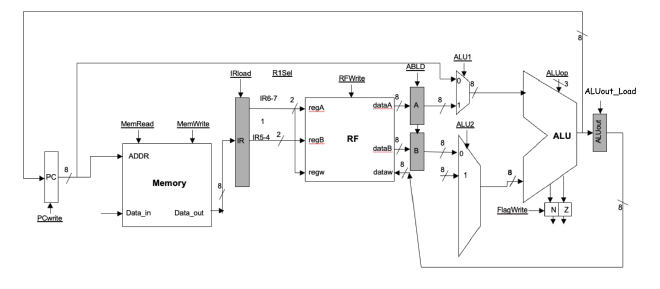
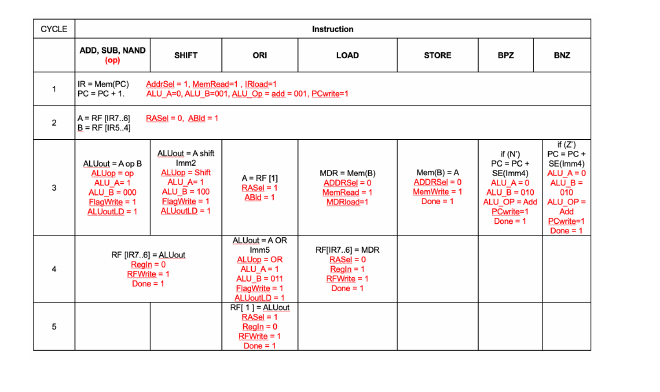
Suppose the add R1, R2 is being coded into 01 10 0100 , which is 0x64 in HEX, and this instruction is stored at address 0x05 , there’ll be six steps for this instruction
- Fetch: Read from memory of what
PCis pointing to, then activateMemReadandIRLoad - Decode: Recognise which instruction is inside
- Read: Read the value of
R1andR2, turn onABld - Compute: Set the
ALUopinto additional mode, and calculateALUout = R1 + R2, the signals areALU_A = 1,ALU_B = 0,ALULoad = 1. After computed, set theZandNbit based on the result (need to enableFlagwrite = 1) - Write: Write back the result of
ALUoutback toRa(RFwrite = 1) - Compute PC: Update the
PC
sub #

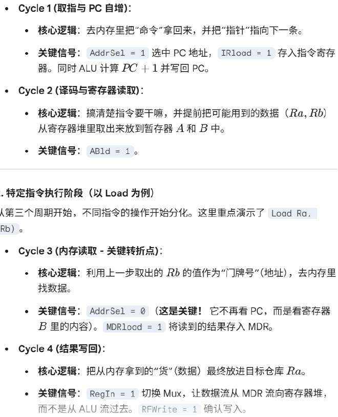
- Fetch and Increment PC:
MemRead=1,PCwrite=1 - Decode & register fetch
- Compute: Use
ALU_Op=001to tell ALU to do subtraction, and store it inALUOut, at the same time, it will update theFlags( zero or negative) - Write:
RFWrite=1
OR Immediate #
Unlike sub , there’s a Immediate Value now, and it requires one more period than sub
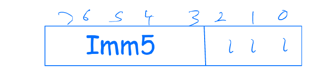
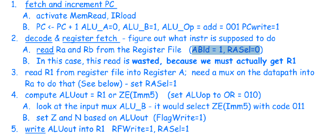
- Fetch: Then same, active
MemRead,IRloadPC <- PC + 1 ALU_A=0, ALU_B=1, ALU_Op = add = 001 PCwrite=1 - Decode & register fetch: Read
RaandRbfrom the Register File
- 这次读取是浪费的 (Wasted)
- 对于
ori指令,我们需要读的是寄存器R1(通常对应编码中的某个位置),而硬件逻辑在这一步还没准备好。
Load #

Store #
BNZ #
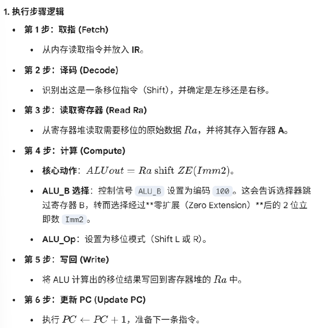
Shift L/R Ra, Imm2 #
FSM Cycles #
Load #
BNZ Imm4 #
Processor elements #
Register File #
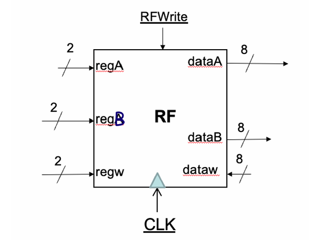
- 通过
regA和regB两个 2-bit 输入信号,分别从dataA和dataB端口同时输出两个 8-bit 数据 - 通过
regw(2-bit)选择目标寄存器,在RFWrite信号有效且时钟CLK到达时,将dataw(8-bit)的数据写入
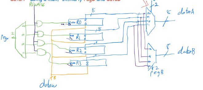
regA信号作为上方 Mux 的选择端,决定dataA输出哪个寄存器的值regB信号作为下方 Mux 的选择端,决定dataB输出哪个寄存器的值- 左侧的 2-bit 输入
regw连接到一个译码器,将其转换为四条选通线(00, 01, 10, 11)。 - 每条选通线与
RFWrite全局信号通过一个 AND 门 相连。 - 使能控制:只有当
RFWrite为 1 且译码器选中该寄存器时,对应寄存器的 Enable(使能) 端才会被激活。 - 数据输入:
dataw(橙色线)连接到所有四个寄存器的输入端,但只有被使能的那个寄存器会在时钟触发时保存该值
ALU #
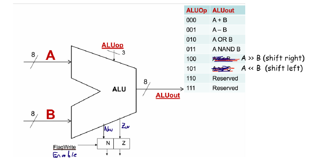
- 输入输出:拥有两个 8-bit 输入端口(A 和 B),一个 8-bit 输出端口(ALUout)。
- 控制信号:
ALUop是一个 3-bit 的选择信号,决定当前的运算类型
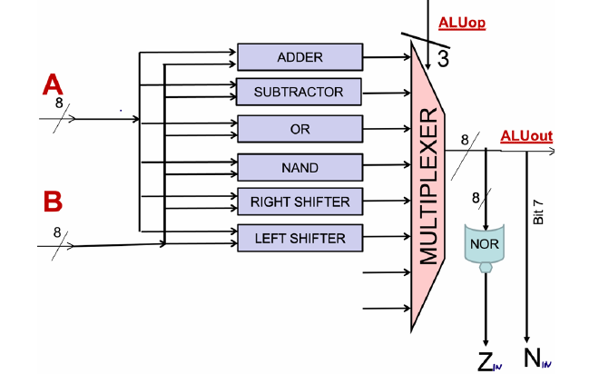
- 并行运算层:输入 A 和 B 同时进入所有的运算模块(加法器、减法器、或门、与非门、移位器)。这意味着所有运算是同时发生的。
ALUop信号连接到 Mux 的选择端。它的作用是从上方所有运算模块的结果中,只选出一个作为最终的ALUout输出
FSM & Memory #
- 读 (
Memread = 1):地址输入后,数据在同一个时钟周期内从DATAout输出。 - 写 (
MemWrite = 1):地址和DATAin输入后,数据在时钟周期结束时完成更改。